U-Boot SPL 2013.01.01 (Oct 12 2016 - 10:38:03)
BOARD : Altera SOCFPGA Cyclone V Board
CLOCK: EOSC1 clock 25000 KHz
CLOCK: EOSC2 clock 25000 KHz
CLOCK: F2S_SDR_REF clock 0 KHz
CLOCK: F2S_PER_REF clock 0 KHz
CLOCK: MPU clock 925 MHz
CLOCK: DDR clock 400 MHz
CLOCK: UART clock 100000 KHz
CLOCK: MMC clock 50000 KHz
CLOCK: QSPI clock 3613 KHz
RESET: COLD
INFO : Watchdog enabled
SDRAM: Initializing MMR registers
SDRAM: Calibrating PHY
SEQ.C: Preparing to start memory calibration
SEQ.C: CALIBRATION PASSED
SDRAM: 1024 MiB
ALTERA DWMMC: 0
U-Boot 2013.01.01 (Oct 12 2016 - 10:40:34)
CPU : Altera SOCFPGA Platform
BOARD : Altera SOCFPGA Cyclone V Board
I2C: ready
DRAM: 1 GiB
MMC: ALTERA DWMMC: 0
*** Warning - bad CRC, using default environment
In: serial
Out: serial
Err: serial
Skipped ethaddr assignment due to invalid EMAC address in EEPROM
Net: mii0
Warning: failed to set MAC address
Hit any key to stop autoboot: 0
reading u-boot.scr
200 bytes read in 3 ms (64.5 KiB/s)
## Executing script at 02000000
reading soc_system.rbf
7007184 bytes read in 327 ms (20.4 MiB/s)
## Starting application at 0x3FF795A4 ...
## Application terminated, rc = 0x0
reading zImage
5538512 bytes read in 259 ms (20.4 MiB/s)
reading socfpga.dtb
31245 bytes read in 5 ms (6 MiB/s)
## Flattened Device Tree blob at 00000100
Booting using the fdt blob at 0x00000100
reserving fdt memory region: addr=0 size=1000
Loading Device Tree to 03ff5000, end 03fffa0c ... OK
Starting kernel ...
[ 0.000000] Booting Linux on physical CPU 0x0
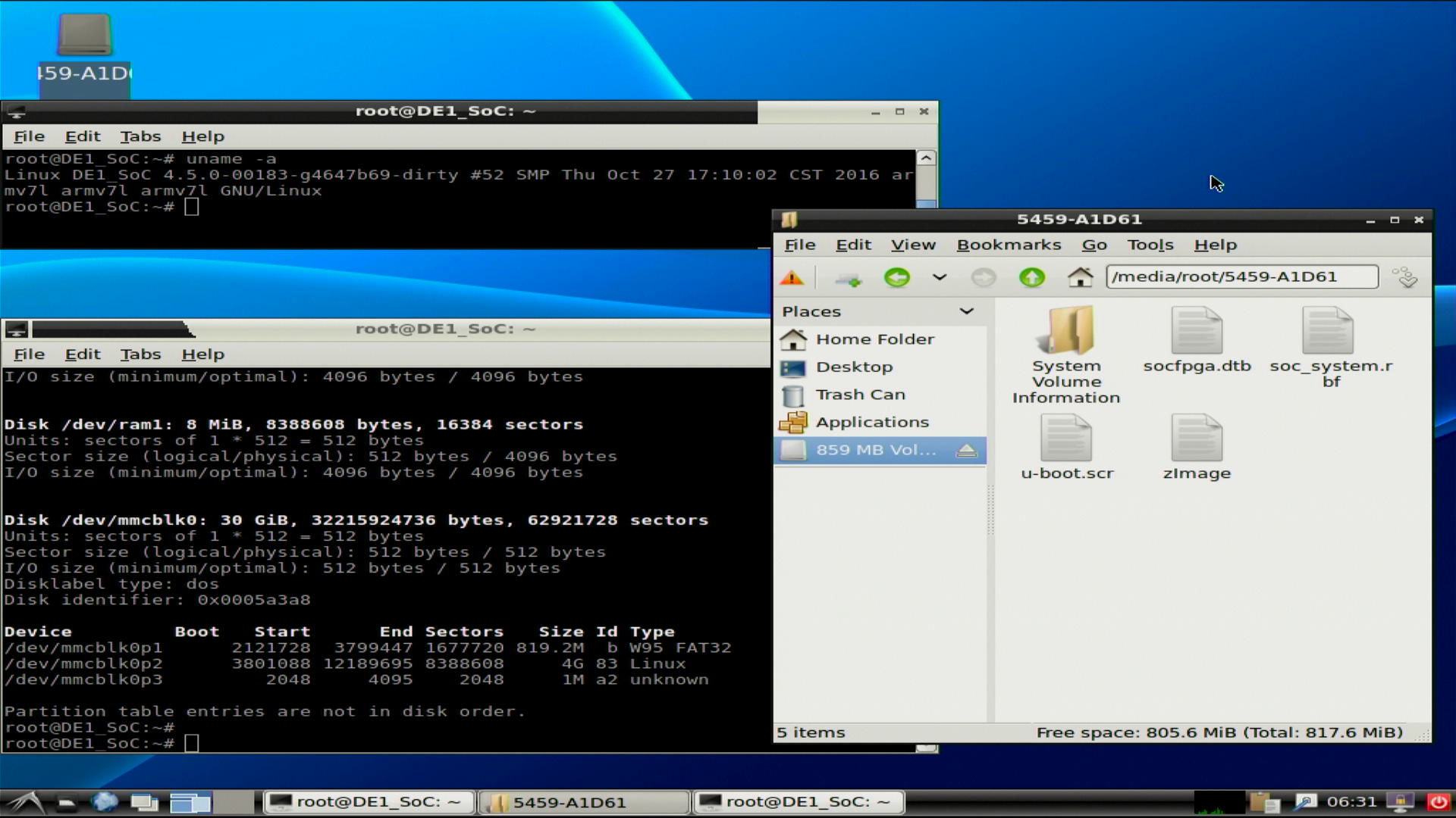
[ 0.000000] Linux version 4.5.0-00183-g4647b69-dirty (root@matthew) (gcc version 4.8.3 20140401 (prerelease) (crosstool-NG linaro-1.13.1-4.8-2014.04 - Linaro GCC 4.8-2014.04) ) #52 SMP Thu Oct 27 17:10:02 CST 2016
[ 0.000000] CPU: ARMv7 Processor [413fc090] revision 0 (ARMv7), cr=10c5387d
[ 0.000000] CPU: PIPT / VIPT nonaliasing data cache, VIPT aliasing instruction cache
[ 0.000000] Machine model: Terasic DE-0(Atlas)
[ 0.000000] Truncating RAM at 0x00000000-0x40000000 to -0x30000000
[ 0.000000] Consider using a HIGHMEM enabled kernel.
[ 0.000000] cma: Reserved 512 MiB at 0x10000000
[ 0.000000] Memory policy: Data cache writealloc
[ 0.000000] PERCPU: Embedded 13 pages/cpu @cf8c3000 s21824 r8192 d23232 u53248
[ 0.000000] Built 1 zonelists in Zone order, mobility grouping on. Total pages: 195072
[ 0.000000] Kernel command line: console=ttyS0,115200 root=/dev/mmcblk0p2 rw rootwait
[ 0.000000] PID hash table entries: 4096 (order: 2, 16384 bytes)
[ 0.000000] Dentry cache hash table entries: 131072 (order: 7, 524288 bytes)
[ 0.000000] Inode-cache hash table entries: 65536 (order: 6, 262144 bytes)
[ 0.000000] Memory: 241776K/786432K available (8614K kernel code, 577K rwdata, 2160K rodata, 600K init, 159K bss, 20368K reserved, 524288K cma-reserved)
[ 0.000000] Virtual kernel memory layout:
[ 0.000000] vector : 0xffff0000 - 0xffff1000 ( 4 kB)
[ 0.000000] fixmap : 0xffc00000 - 0xfff00000 (3072 kB)
[ 0.000000] vmalloc : 0xf0800000 - 0xff800000 ( 240 MB)
[ 0.000000] lowmem : 0xc0000000 - 0xf0000000 ( 768 MB)
[ 0.000000] modules : 0xbf000000 - 0xc0000000 ( 16 MB)
[ 0.000000] .text : 0xc0008000 - 0xc0a8db9c (10775 kB)
[ 0.000000] .init : 0xc0a8e000 - 0xc0b24000 ( 600 kB)
[ 0.000000] .data : 0xc0b24000 - 0xc0bb46fc ( 578 kB)
[ 0.000000] .bss : 0xc0bb46fc - 0xc0bdc524 ( 160 kB)
[ 0.000000] SLUB: HWalign=64, Order=0-3, MinObjects=0, CPUs=2, Nodes=1
[ 0.000000] Hierarchical RCU implementation.
[ 0.000000] Build-time adjustment of leaf fanout to 32.
[ 0.000000] NR_IRQS:16 nr_irqs:16 16
[ 0.000000] L2C: platform modifies aux control register: 0x02060000 -> 0x32460000
[ 0.000000] L2C: platform provided aux values permit register corruption.
[ 0.000000] L2C: DT/platform modifies aux control register: 0x02060000 -> 0x32460000
[ 0.000000] L2C-310 erratum 769419 enabled
[ 0.000000] L2C-310 enabling early BRESP for Cortex-A9
[ 0.000000] L2C-310 full line of zeros enabled for Cortex-A9
[ 0.000000] L2C-310 ID prefetch enabled, offset 1 lines
[ 0.000000] L2C-310 dynamic clock gating enabled, standby mode enabled
[ 0.000000] L2C-310 cache controller enabled, 8 ways, 512 kB
[ 0.000000] L2C-310: CACHE_ID 0x410030c9, AUX_CTRL 0x76460001
[ 0.000000] clocksource: timer1: mask: 0xffffffff max_cycles: 0xffffffff, max_idle_ns: 19112604467 ns
[ 0.000005] sched_clock: 32 bits at 100MHz, resolution 10ns, wraps every 21474836475ns
[ 0.000016] Switching to timer-based delay loop, resolution 10ns
[ 0.000311] Console: colour dummy device 80x30
[ 0.000329] Calibrating delay loop (skipped), value calculated using timer frequency.. 200.00 BogoMIPS (lpj=1000000)
[ 0.000341] pid_max: default: 32768 minimum: 301
[ 0.000427] Mount-cache hash table entries: 2048 (order: 1, 8192 bytes)
[ 0.000437] Mountpoint-cache hash table entries: 2048 (order: 1, 8192 bytes)
[ 0.000941] CPU: Testing write buffer coherency: ok
[ 0.000969] ftrace: allocating 26820 entries in 79 pages
[ 0.041869] CPU0: thread -1, cpu 0, socket 0, mpidr 80000000
[ 0.042092] Setting up static identity map for 0x8280 - 0x82d8
[ 0.043433] CPU1: thread -1, cpu 1, socket 0, mpidr 80000001
[ 0.043494] Brought up 2 CPUs
[ 0.043508] SMP: Total of 2 processors activated (400.00 BogoMIPS).
[ 0.043513] CPU: All CPU(s) started in SVC mode.
[ 0.044174] devtmpfs: initialized
[ 0.050496] VFP support v0.3: implementor 41 architecture 3 part 30 variant 9 rev 4
[ 0.050777] clocksource: jiffies: mask: 0xffffffff max_cycles: 0xffffffff, max_idle_ns: 19112604462750000 ns
[ 0.074717] NET: Registered protocol family 16
[ 0.083918] DMA: preallocated 4096 KiB pool for atomic coherent allocations
[ 0.090177] hw-breakpoint: found 5 (+1 reserved) breakpoint and 1 watchpoint registers.
[ 0.090191] hw-breakpoint: maximum watchpoint size is 4 bytes.
[ 0.121529] SCSI subsystem initialized
[ 0.121788] usbcore: registered new interface driver usbfs
[ 0.121847] usbcore: registered new interface driver hub
[ 0.121909] usbcore: registered new device driver usb
[ 0.122039] soc:usbphy@0 supply vcc not found, using dummy regulator
[ 0.122789] media: Linux media interface: v0.10
[ 0.122847] Linux video capture interface: v2.00
[ 0.122899] pps_core: LinuxPPS API ver. 1 registered
[ 0.122906] pps_core: Software ver. 5.3.6 - Copyright 2005-2007 Rodolfo Giometti <giometti@linux.it>
[ 0.122932] PTP clock support registered
[ 0.123089] FPGA manager framework
[ 0.123660] Bluetooth: Core ver 2.21
[ 0.123710] NET: Registered protocol family 31
[ 0.123717] Bluetooth: HCI device and connection manager initialized
[ 0.123732] Bluetooth: HCI socket layer initialized
[ 0.123743] Bluetooth: L2CAP socket layer initialized
[ 0.123768] Bluetooth: SCO socket layer initialized
[ 0.125402] clocksource: Switched to clocksource timer1
[ 0.173018] NET: Registered protocol family 2
[ 0.173512] TCP established hash table entries: 8192 (order: 3, 32768 bytes)
[ 0.173589] TCP bind hash table entries: 8192 (order: 4, 65536 bytes)
[ 0.173695] TCP: Hash tables configured (established 8192 bind 8192)
[ 0.173770] UDP hash table entries: 512 (order: 2, 16384 bytes)
[ 0.173814] UDP-Lite hash table entries: 512 (order: 2, 16384 bytes)
[ 0.174000] NET: Registered protocol family 1
[ 0.174331] RPC: Registered named UNIX socket transport module.
[ 0.174340] RPC: Registered udp transport module.
[ 0.174346] RPC: Registered tcp transport module.
[ 0.174351] RPC: Registered tcp NFSv4.1 backchannel transport module.
[ 0.175514] futex hash table entries: 512 (order: 3, 32768 bytes)
[ 0.184446] NFS: Registering the id_resolver key type
[ 0.184495] Key type id_resolver registered
[ 0.184502] Key type id_legacy registered
[ 0.184563] ntfs: driver 2.1.32 [Flags: R/W].
[ 0.184838] jffs2: version 2.2. (NAND) © 2001-2006 Red Hat, Inc.
[ 0.185430] SGI XFS with ACLs, security attributes, no debug enabled
[ 0.189606] io scheduler noop registered (default)
[ 0.211937] Console: switching to colour frame buffer device 128x48
[ 0.224086] altvipfb ff200100.vip2: fb0: altvipfb frame buffer device at 0x10400000+0x300000
[ 0.227906] Serial: 8250/16550 driver, 2 ports, IRQ sharing disabled
[ 0.228925] console [ttyS0] disabled
[ 0.228966] ffc02000.serial0: ttyS0 at MMIO 0xffc02000 (irq = 39, base_baud = 6250000) is a 16550A
[ 0.852835] console [ttyS0] enabled
[ 0.856932] ffc03000.serial1: ttyS1 at MMIO 0xffc03000 (irq = 40, base_baud = 6250000) is a 16550A
[ 0.867533] brd: module loaded
[ 0.872162] CAN device driver interface
[ 0.876535] stmmac - user ID: 0x10, Synopsys ID: 0x37
[ 0.881569] Ring mode enabled
[ 0.884608] DMA HW capability register supported
[ 0.889135] Enhanced/Alternate descriptors
[ 0.893481] Enabled extended descriptors
[ 0.897480] RX Checksum Offload Engine supported (type 2)
[ 0.902938] TX Checksum insertion supported
[ 0.907195] Enable RX Mitigation via HW Watchdog Timer
[ 0.912913] socfpga-dwmac ff702000.ethernet eth0: No MDIO subnode found
[ 0.925033] libphy: stmmac: probed
[ 0.928449] eth0: PHY ID 00221611 at 1 IRQ POLL (stmmac-0:01) active
[ 0.935262] ffb40000.usb supply vusb_d not found, using dummy regulator
[ 0.941921] ffb40000.usb supply vusb_a not found, using dummy regulator
[ 1.225353] dwc2 ffb40000.usb: EPs: 16, dedicated fifos, 8064 entries in SPRAM
[ 1.325742] dwc2 ffb40000.usb: DWC OTG Controller
[ 1.330452] dwc2 ffb40000.usb: new USB bus registered, assigned bus number 1
[ 1.337516] dwc2 ffb40000.usb: irq 41, io mem 0x00000000
[ 1.343072] usb usb1: New USB device found, idVendor=1d6b, idProduct=0002
[ 1.349848] usb usb1: New USB device strings: Mfr=3, Product=2, SerialNumber=1
[ 1.357047] usb usb1: Product: DWC OTG Controller
[ 1.361732] usb usb1: Manufacturer: Linux 4.5.0-00183-g4647b69-dirty dwc2_hsotg
[ 1.369016] usb usb1: SerialNumber: ffb40000.usb
[ 1.374165] hub 1-0:1.0: USB hub found
[ 1.377947] hub 1-0:1.0: 1 port detected
[ 1.382544] usbcore: registered new interface driver usb-storage
[ 1.388912] mousedev: PS/2 mouse device common for all mice
[ 1.394776] i2c /dev entries driver
[ 1.398719] usbcore: registered new interface driver uvcvideo
[ 1.404442] USB Video Class driver (1.1.1)
[ 1.408544] gspca_main: v2.14.0 registered
[ 1.412684] usbcore: registered new interface driver benq
[ 1.418129] usbcore: registered new interface driver conex
[ 1.423641] usbcore: registered new interface driver cpia1
[ 1.429166] usbcore: registered new interface driver dtcs033
[ 1.434849] usbcore: registered new interface driver etoms
[ 1.440374] usbcore: registered new interface driver finepix
[ 1.446081] usbcore: registered new interface driver jeilinj
[ 1.451767] usbcore: registered new interface driver jl2005bcd
[ 1.457660] usbcore: registered new interface driver kinect
[ 1.463259] usbcore: registered new interface driver konica
[ 1.468869] usbcore: registered new interface driver mars
[ 1.474306] usbcore: registered new interface driver mr97310a
[ 1.480114] usbcore: registered new interface driver nw80x
[ 1.485665] usbcore: registered new interface driver ov519
[ 1.491179] usbcore: registered new interface driver ov534
[ 1.496707] usbcore: registered new interface driver ov534_9
[ 1.502407] usbcore: registered new interface driver pac207
[ 1.508022] usbcore: registered new interface driver gspca_pac7302
[ 1.514224] usbcore: registered new interface driver pac7311
[ 1.519924] usbcore: registered new interface driver se401
[ 1.525458] usbcore: registered new interface driver sn9c2028
[ 1.531234] usbcore: registered new interface driver gspca_sn9c20x
[ 1.537453] usbcore: registered new interface driver sonixb
[ 1.543055] usbcore: registered new interface driver sonixj
[ 1.548667] usbcore: registered new interface driver spca500
[ 1.554350] usbcore: registered new interface driver spca501
[ 1.560046] usbcore: registered new interface driver spca505
[ 1.565743] usbcore: registered new interface driver spca506
[ 1.571427] usbcore: registered new interface driver spca508
[ 1.577134] usbcore: registered new interface driver spca561
[ 1.582820] usbcore: registered new interface driver spca1528
[ 1.588610] usbcore: registered new interface driver sq905
[ 1.594122] usbcore: registered new interface driver sq905c
[ 1.599737] usbcore: registered new interface driver sq930x
[ 1.605354] usbcore: registered new interface driver sunplus
[ 1.611038] usbcore: registered new interface driver stk014
[ 1.616648] usbcore: registered new interface driver stk1135
[ 1.622338] usbcore: registered new interface driver stv0680
[ 1.628038] usbcore: registered new interface driver t613
[ 1.633477] usbcore: registered new interface driver gspca_topro
[ 1.639522] usbcore: registered new interface driver touptek
[ 1.645202] usbcore: registered new interface driver tv8532
[ 1.650813] usbcore: registered new interface driver vc032x
[ 1.656422] usbcore: registered new interface driver vicam
[ 1.661949] usbcore: registered new interface driver xirlink-cit
[ 1.668019] usbcore: registered new interface driver gspca_zc3xx
[ 1.674066] usbcore: registered new interface driver ALi m5602
[ 1.679952] usbcore: registered new interface driver STV06xx
[ 1.685663] usbcore: registered new interface driver gspca_gl860
[ 1.692422] Bluetooth: HCI UART driver ver 2.3
[ 1.696882] Bluetooth: HCI UART protocol H4 registered
[ 1.701998] Bluetooth: HCI UART protocol BCSP registered
[ 1.707334] Bluetooth: HCI UART protocol LL registered
[ 1.712452] Bluetooth: HCI UART protocol ATH3K registered
[ 1.717848] Bluetooth: HCI UART protocol Three-wire (H5) registered
[ 1.724164] Bluetooth: HCI UART protocol Intel registered
[ 1.729624] Bluetooth: HCI UART protocol BCM registered
[ 1.734829] Bluetooth: HCI UART protocol QCA registered
[ 1.740146] usbcore: registered new interface driver bcm203x
[ 1.745897] usbcore: registered new interface driver bpa10x
[ 1.751512] usbcore: registered new interface driver bfusb
[ 1.757078] usbcore: registered new interface driver btusb
[ 1.762548] Bluetooth: Generic Bluetooth SDIO driver ver 0.1
[ 1.768296] Synopsys Designware Multimedia Card Interface Driver
[ 1.774581] dw_mmc ff704000.dwmmc0: IDMAC supports 32-bit address mode.
[ 1.781394] dw_mmc ff704000.dwmmc0: Using internal DMA controller.
[ 1.787583] dw_mmc ff704000.dwmmc0: Version ID is 240a
[ 1.792741] dw_mmc ff704000.dwmmc0: DW MMC controller at irq 30,32 bit host data width,1024 deep fifo
[ 1.835392] dw_mmc ff704000.dwmmc0: 1 slots initialized
[ 1.841009] ledtrig-cpu: registered to indicate activity on CPUs
[ 1.847224] usbcore: registered new interface driver usbhid
[ 1.852773] usbhid: USB HID core driver
[ 1.856833] fpga_manager fpga0: Altera SOCFPGA FPGA Manager registered
[ 1.863818] altera_hps2fpga_bridge ff400000.fpga-bridge: fpga bridge [lwhps2fpga] registered
[ 1.872466] altera_hps2fpga_bridge ff500000.fpga-bridge: fpga bridge [hps2fpga] registered
[ 1.880947] altera_hps2fpga_bridge ff600000.fpga-bridge: fpga bridge [fpga2hps] registered
[ 1.889675] altera_fpga2sdram_bridge soc:fpga2sdram-bridge: fpga bridge [fpga2sdram] registered
[ 1.898357] altera_fpga2sdram_bridge soc:fpga2sdram-bridge: driver initialized with handoff 00000000
[ 1.907794] fpga-region soc:base-fpga-region: FPGA Region probed
[ 1.914046] oprofile: no performance counters
[ 1.918508] oprofile: using timer interrupt.
[ 1.923835] NET: Registered protocol family 10
[ 1.929063] sit: IPv6 over IPv4 tunneling driver
[ 1.934268] NET: Registered protocol family 17
[ 1.938743] NET: Registered protocol family 15
[ 1.943172] can: controller area network core (rev 20120528 abi 9)
[ 1.949389] NET: Registered protocol family 29
[ 1.953821] can: raw protocol (rev 20120528)
[ 1.958089] can: broadcast manager protocol (rev 20120528 t)
[ 1.963731] can: netlink gateway (rev 20130117) max_hops=1
[ 1.969497] Bluetooth: RFCOMM TTY layer initialized
[ 1.974374] Bluetooth: RFCOMM socket layer initialized
[ 1.979523] Bluetooth: RFCOMM ver 1.11
[ 1.983271] Bluetooth: BNEP (Ethernet Emulation) ver 1.3
[ 1.988582] Bluetooth: BNEP filters: protocol multicast
[ 1.993792] Bluetooth: BNEP socket layer initialized
[ 1.998756] Bluetooth: HIDP (Human Interface Emulation) ver 1.2
[ 2.004655] Bluetooth: HIDP socket layer initialized
[ 2.009666] 8021q: 802.1Q VLAN Support v1.8
[ 2.013867] lib80211: common routines for IEEE802.11 drivers
[ 2.019591] Key type dns_resolver registered
[ 2.023943] ThumbEE CPU extension supported.
[ 2.028223] Registering SWP/SWPB emulation handler
[ 2.034119] of_cfs_init
[ 2.036666] of_cfs_init: OK
[ 2.041328] Bluetooth: Starting self testing
[ 2.085351] usb 1-1: new high-speed USB device number 2 using dwc2
[ 2.097751] Bluetooth: ECDH test passed in 50876 usecs
[ 2.103948] Bluetooth: SMP test passed in 134 usecs
[ 2.108870] Bluetooth: Finished self testing
[ 2.113431] ttyS0 - failed to request DMA
[ 2.117487] mmc_host mmc0: Bus speed (slot 0) = 50000000Hz (slot req 50000000Hz, actual 50000000HZ div = 0)
[ 2.117520] Waiting for root device /dev/mmcblk0p2...
[ 2.132287] mmc0: new high speed SDHC card at address b36c
[ 2.138252] mmcblk0: mmc0:b36c SDABC 30.0 GiB
[ 2.143713] mmcblk0: p1 p2 p3
[ 2.225780] EXT4-fs (mmcblk0p2): couldn't mount as ext3 due to feature incompatibilities
[ 2.295525] usb 1-1: New USB device found, idVendor=0424, idProduct=2512
[ 2.302206] usb 1-1: New USB device strings: Mfr=0, Product=0, SerialNumber=0
[ 2.309957] hub 1-1:1.0: USB hub found
[ 2.313816] hub 1-1:1.0: 2 ports detected
[ 2.450577] EXT4-fs (mmcblk0p2): recovery complete
[ 2.456318] EXT4-fs (mmcblk0p2): mounted filesystem with ordered data mode. Opts: (null)
[ 2.464400] VFS: Mounted root (ext4 filesystem) on device 179:2.
[ 2.477897] devtmpfs: mounted
[ 2.481304] Freeing unused kernel memory: 600K (c0a8e000 - c0b24000)
[ 2.700821] systemd[1]: System time before build time, advancing clock.
[ 2.721925] systemd[1]: Failed to insert module 'autofs4': No such file or directory
[ 2.750264] random: systemd urandom read with 58 bits of entropy available
[ 2.759785] systemd[1]: systemd 229 running in system mode. (+PAM +AUDIT +SELINUX +IMA +APPARMOR +SMACK +SYSVINIT +UTMP +LIBCRYPTSETUP +GCRYPT +GNUTLS +ACL +XZ -LZ4 +SECCOMP +BLKID +ELFUTILS +KMOD -IDN)
[ 2.778156] systemd[1]: Detected architecture arm.
Welcome to Ubuntu 16.04.1 LTS!
[ 2.816078] systemd[1]: Set hostname to <DE1_SoC>.
[ 3.207584] systemd[1]: Listening on Journal Socket.
[ OK ] Listening on Journal Socket.
[ 3.225650] systemd[1]: Listening on Syslog Socket.
[ OK ] Listening on Syslog Socket.
[ 3.245557] systemd[1]: Listening on udev Kernel Socket.
[ OK ] Listening on udev Kernel Socket.
[ 3.265561] systemd[1]: Listening on Journal Socket (/dev/log).
[ OK ] Listening on Journal Socket (/dev/log).
[ 3.285724] systemd[1]: Listening on /dev/initctl Compatibility Named Pipe.
[ OK ] Listening on /dev/initctl Compatibility Named Pipe.
[ 3.305561] systemd[1]: Reached target Remote File Systems (Pre).
[ OK ] Reached target Remote File Systems (Pre).
[ 3.325467] systemd[1]: Reached target Swap.
[ OK ] Reached target Swap.
[ 3.345613] systemd[1]: Listening on udev Control Socket.
[ OK ] Listening on udev Control Socket.
[ 3.365471] systemd[1]: Reached target Encrypted Volumes.
[ OK ] Reached target Encrypted Volumes.
[ 3.385651] systemd[1]: Created slice User and Session Slice.
[ OK ] Created slice User and Session Slice.
[ 3.416756] systemd[1]: Reached target Remote File Systems.
[ OK ] Reached target Remote File Systems.
[ 3.435713] systemd[1]: Created slice System Slice.
[ OK ] Created slice System Slice.
[ 3.485790] systemd[1]: Starting Nameserver information manager...
Starting Nameserver information manager...
[ 3.507481] systemd[1]: Starting Journal Service...
Starting Journal Service...
[ 3.576219] systemd[1]: Starting Load Kernel Modules...
Starting Load Kernel Modules...
[ 3.597416] systemd[1]: Mounting Debug File System...
Mounting Debug File System...
[ 3.617216] systemd[1]: Starting Set console keymap...
Starting Set console keymap...
[ 3.647681] systemd[1]: Starting Remount Root and Kernel File Systems...
Starting Remount Root and Kernel File Systems...
[ 3.675946] systemd[1]: Created slice system-serial\x2dgetty.slice.
[ OK ] Created slice system-serial\x2dgetty.slice.
[ 3.695782] systemd[1]: Reached target User and Group Name Lookups.
[ OK ] Reached target User and Group Name Lookups.
[ 3.715593] systemd[1]: Reached target Slices.
[ OK ] Reached target Slices.
[ 3.735763] systemd[1]: Started Forward Password Requests to Wall Directory Watch.
[ OK ] Started Forward Password Requests to Wall Directory Watch.
[ 3.815900] systemd[1]: Starting Create Static Device Nodes in /dev...
Starting Create Static Device Nodes in /dev...
[ 3.837510] systemd[1]: Started Read required files in advance.
[ OK ] Started Read required files in advance.
[ 3.871472] systemd[1]: Mounted Debug File System.
[ OK ] Mounted Debug File System.
[ 3.904989] systemd[1]: Started Journal Service.
[ OK ] Started Journal Service.
[ OK ] Started Load Kernel Modules.
[ OK ] Started Set console keymap.
[ OK ] Started Remount Root and Kernel File Systems.
[ OK ] Started Create Static Device Nodes in /dev.
[ OK ] Started Nameserver information manager.
Starting udev Kernel Device Manager...
Starting udev Coldplug all Devices...
Starting Load/Save Random Seed...
[ OK ] Reached target Local File Systems (Pre).
[ OK ] Reached target Local File Systems.
Starting Set console font and keymap...
Starting Tell Plymouth To Write Out Runtime Data...
Mounting Configuration File System...
Starting Apply Kernel Variables...
Starting Flush Journal to Persistent Storage...
[ OK ] Mounted Configuration File System.
[ OK ] Started Load/Save Random Seed.
[ OK ] Started Tell Plymouth To Write Out Runtime Data.
[ OK ] Started Apply Kernel Variables.
[ OK ] Started udev Kernel Device Manager.
[ OK ] Started Flush Journal to Persistent Storage.
[ OK ] Started udev Coldplug all Devices.
Starting Create Volatile Files and Directories...
[ OK ] Started Dispatch Password Requests to Console Directory Watch.
Starting Raise network interfaces...
[ OK ] Started Create Volatile Files and Directories.
Starting Network Time Synchronization...
Starting Update UTMP about System Boot/Shutdown...
[ OK ] Started Update UTMP about System Boot/Shutdown.
[ OK ] Started Network Time Synchronization.
[ OK ] Reached target System Time Synchronized.
[ OK ] Reached target System Initialization.
[ OK ] Started Trigger resolvconf update for networkd DNS.
[ OK ] Listening on ACPID Listen Socket.
[ OK ] Started ACPI Events Check.
[ OK ] Reached target Paths.
[ OK ] Listening on Avahi mDNS/DNS-SD Stack Activation Socket.
[ OK ] Listening on D-Bus System Message Bus Socket.
[ OK ] Reached target Sockets.
[ OK ] Reached target Basic System.
Starting Generic Board Startup...
Starting LSB: Set the CPU Frequency Scaling governor to "ondemand"...
[ OK ] Started Regular background program processing daemon.
Starting Permit User Sessions...
Starting Restore /etc/resolv.conf i...re the ppp link was shut down...
Starting Avahi mDNS/DNS-SD Stack...
[ OK ] Started ACPI event daemon.
Starting System Logging Service...
Starting Accounts Service...
Starting LSB: Start busybox udhcpd at boot time...
[ OK ] Started D-Bus System Message Bus.
[ OK ] Started Avahi mDNS/DNS-SD Stack.
Starting Modem Manager...
Starting Network Manager...
[ OK ] Started Daily apt activities.
[ OK ] Started Daily Cleanup of Temporary Directories.
[ OK ] Reached target Timers.
Starting Login Service...
Starting Cape Manager Service...
Starting LSB: Load kernel modules needed to enable cpufreq scaling...
[ OK ] Started System Logging Service.
[ OK ] Started Set console font and keymap.
[ OK ] Started Generic Board Startup.
[ OK ] Started Permit User Sessions.
[ OK ] Started Restore /etc/resolv.conf if...fore the ppp link was shut down.
[ OK ] Started Cape Manager Service.
[ OK ] Found device /dev/ttyS0.
[ OK ] Started LSB: Set the CPU Frequency Scaling governor to "ondemand".
[ OK ] Started LSB: Start busybox udhcpd at boot time.
[ OK ] Started Network Manager.
[ OK ] Started Login Service.
Starting Network Manager Script Dispatcher Service...
Starting Network Manager Wait Online...
Starting Authenticate and Authorize Users to Run Privileged Tasks...
[ OK ] Started ifup for eth0.
Starting Light Display Manager...
[ OK ] Created slice system-getty.slice.
[ OK ] Started LSB: Load kernel modules needed to enable cpufreq scaling.
[ OK ] Started Network Manager Script Dispatcher Service.
[ OK ] Started Authenticate and Authorize Users to Run Privileged Tasks.
[ OK ] Started Accounts Service.
[ OK ] Started Modem Manager.
Starting Hostname Service...
Starting LSB: set CPUFreq kernel parameters...
[ OK ] Started Light Display Manager.
[ OK ] Started Hostname Service.
[ OK ] Started LSB: set CPUFreq kernel parameters.
[ OK ] Created slice User Slice of root.
Starting User Manager for UID 0...
[ OK ] Started Session c1 of user root.
[ OK ] Started User Manager for UID 0.
Starting Disk Manager...
[ OK ] Started Disk Manager.
[ OK ] Started Network Manager Wait Online.
[FAILED] Failed to start Raise network interfaces.
See 'systemctl status networking.service' for details.
[ OK ] Reached target Network.
Starting OpenBSD Secure Shell server...
[ OK ] Reached target Network is Online.
Starting LSB: Advanced IEEE 802.11 management daemon...
Starting LSB: Apache2 web server...
Starting /etc/rc.local Compatibility...
[ OK ] Started LSB: Advanced IEEE 802.11 management daemon.
[ OK ] Started /etc/rc.local Compatibility.
Starting Hold until boot process finishes up...
[ OK ] Started Hold until boot process finishes up.
[ OK ] Started Getty on tty1.
Starting Set console scheme...
[ OK ] Started Serial Getty on ttyS0.
[ OK ] Reached target Login Prompts.
[ OK ] Started Set console scheme.
[ OK ] Started LSB: Apache2 web server.
[ OK ] Started OpenBSD Secure Shell server.
[ OK ] Reached target Multi-User System.
[ OK ] Reached target Graphical Interface.
Starting Update UTMP about System Runlevel Changes...
[ OK ] Started Stop ureadahead data collection 45s after completed startup.
[ OK ] Started Update UTMP about System Runlevel Changes.
Ubuntu 16.04.1 LTS DE1_SoC ttyS0
default username:password is [ubuntu:temppwd]
DE1_SoC login: |